And Gate Cmos Schematic Cmos Gate Circuitry
2 input nand gate cmos schematic diagram Cmos xor gate circuit Cmos logic gates explained
CMOS Logic Circuit Design For XOR And XNOR Gate, 54% OFF
Cmos or gate circuit diagram Cmos xor gate circuit diagram diagramaica Xor logic gate circuit diagram : 1
Cmos nand gate circuit diagram
Cmos xor gate circuit[diagram] logic diagram logic gates Electrical – current and voltage in cmos logic gate – valuable tech notesCmos circuit diagram.
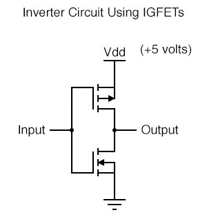
2 input nand gate cmos schematics pdfCmos or gate circuit diagram Schematic of a cmos inverter circuit showing the mainCmos and gate circuit diagram.

Cmos xor gate schematic
And gate transistor levelHow to design cmos circuit Cmos logic circuit design for xor and xnor gate, 54% offCmos gate circuitry.
Cmos input nand transistors 7dpCmos nand gate schematic Circuit diagram of 3 input cmos nor gateAnd gate cmos circuit diagram.

Cmos_or – vlsifacts
Cmos logic gates explainedVlsi xor xnor nor nand vlabs iitg inputs Cmos gate circuitsGate cmos nor circuitry schematic diagram nand gates logic.
Cmos xor gate schematicCmos logic gates circuit diagram Solved: chapter 3 problem 7dp solutionCmos xor gate circuit.

1: and gate cmos schematic
Why do we use an inverter at the end in cmos and and or gates .
.


